IoE (Institute of Engineering)

The Institute of Engineering, established in 1930, is the first technical school of Nepal. It was reformed in the present shape in 1972 as an organ of Tribhuvan University. Besides producing low and tertiary level technicians, IOE runs professional diplomas, undergraduate, postgraduate and Ph.D. programs.

Electrical Club Members of NCE

IOE ELECTRICAL CLUB is the team of electrical students studying at IOE. The group was established to fascilate the students to share their ideas regarding electrical technology and electrical projects. The club helps students to support and guide the projects in which they are engaged in

Various Sports Awards

The Nepal national basketball team represents Nepal in international basketball competitions and is managed by the NCE College.

Wireless Electric Vehicle Charging Technology

Wireless electricity is quite literally the transmission of electrical energy without wires.The principle behind the Tesla coil is to achieve a phenomenon called resonance.The massive amount of energy makes the magnetic field collapse quickly, and generates an electric current in the secondary coil.

Winner

“No man needs sympathy because he has to work, because he has a burden to carry. Far and away the best prize that life offers is the chance to work hard at work worth doing.”

Showing posts with label EEM. Show all posts

Electrical Engineering Material Question Bank solution pdf IOE All Subject Note pdf


Electrical Engineering Material  Question Bank solution


IOE Electrical Engineering Material OLD Question solutions of IOE Regular and Back Questions with short theory important numerical as well as derivations are included here . Strictly in this page you can read electrical engineering notes for 3rd semester as pulchowk campus engineering notes . Here you will find ioe old question answers that are asked in ioe final examination of electrical engineering material according to ioe syllabus for electrical engineering material (EE502) 
IOE ALL SUBJECT NOTES

Chapter 1 : Theory of Metal

Define population density

If we multiply density of state Z(E) & probability of occupation index F(E) then we obtain the number of electrons (per unit energy) per unit volume which is denoted by nE & is called population density.

OR

( If we multiply density of states Z(E) and probability of occupation F(E) then we will get number of electrons occupied in a state i.e. nE and is called population density.)

 Thermionic Emission

When a metal is heated the electron within it becomes highly energetic and gets ejected from its surface . This process of ejection of electron from metal surface at high temperature is called as thermionic  emission.

Work function

There is a minimum (threshold) value of energy that the electron must posses if it is to leave the metal surface. This threshold value of energy is called work function of the metal(ɸ).

Schottky Effect

When an electric field applied to a metal is increased, the work function is decreased and hence thermionic emission from the metal surface increases. This effect is called Schottky effect.

Explain the necessity of quantum mechanics.

  1. To understand the tunneling phenomena.
  2. To understand the photoelectric effect.
  3. To understand the behavior or nature of microscopic particles or electrons.


Chapter 2 : Free Electron Theory of Conduction in Metal


Free Electron Theory Electrical Engineering Material


Crystalline Structure: 

It is an periodic arrangement of atoms( or molecules) in a regular pattern in space. It is the combination of lattice and basis where lattice is the infinite periodic arrangement of points in space and basis is the pair of atoms or molecules when these basis occupy the points of a lattice then we get a crystal structure.

Unit cell: 

It is the simplest structure obtained from the crystal structure. When we extend the unit cell structure in all directions in space then we get a crystal structure.

Co-ordination Number : 

It is the number of nearest neighboring atoms or the number of atoms touching the largest atom of a unit cell.

Packing density: 

It is the ratio of volume occupied by atoms to the volume of unit cell. It signifies how densely the atoms are packed in the unit cell.

Latice parameter : 
a, α ,β ,𝛄


IOE 2074 Ashwin Electrical Engineering Material Old Question Solution


1.a). Explain the importance of quantum mechanics. Differentiate between classical and quantum mechanics with suitable examples.


Ans: The importance of quantum mechanics are listed below:-
  • To understand the tunneling phenomena.
  • To understand the photoelectric effect.
  • To understand the nature of microscopic particles.
  • Quantum mechanics is a generalized form of mechanics which is applicable to very small object like electrons in the atom.
  • All the electronic phenomena within the materials can not be explained with the help of the classical mechanics rather explained by quantum mechanics.
Difference between  classical and quantum mechanics are given below :- 

Classical Mechanics
  1. It can be applied to macroscopic bodies.
  2. It is based on Newton's law of motion.
  3. The state of a system is defined by specifying all the forces acting on the particles as well as their position and velocity. The future state then can be predicted with certainty.
  4. It is based on Maxwell's electromagnetic wave theory. 
Quantum Mechanics
  1. It can be applied to microscopic bodies.
  2. It follow Heisenberg Uncertainty principal.
  3. It gives the probability of finding the particles at various location in space.
  4. It is based on plank's quantum theory.


IOE 2068 Shrawan Electrical Engineering Material Past question solution

1.a) What is tunneling phenomenon? Derive the expression for the probability of tunneling the potential barrier of width L and height V by electron.


Ans: Tunneling phenomenon: Tunneling is a quantum mechanical phenomena such that an electron or wave can penetrate a potential barrier and appear at another region. This is possible only if the potential barrier is relatively lower and width of potential barrier is relatively narrower. 

Fermi Energy: 

In metal fermi energy is defined as the energy of highest filled energy level at temperature of absolute zero .

Share:

Electrical Engineering material ioe notes very important questions and answers

 Electrical Engineering material(ii/i) ioe ALL SUBJECT NOTE  notes
https://notepulchowkcampus.blogspot.com/
Download this note in pdf format Click on Download 

https://notepulchowkcampus.blogspot.com/

Extrinsic Semiconductor

The conductivity of semiconductor risen when some element belonging to either group iii or group v in Mendeleev periodic table are added on it. These elements are called impurities. The extrinsic semiconductors doped with these impurities is called extrinsic semiconductor. These conductor are of two type :

  1. 1.       P- Type semiconductor
  2. 2.       N- Type semiconductor

N –Type semiconductor:

When a pentavalent impurity like Arsenic, Potassium, and Antimony is added to a pure semiconductor a n-type semiconductor is formed. The four electrons out of five valance electron of these impurities make covalent bond with four valance electron of si so one electron remains free on every add of impurities. This extra electron continuously revolves around the impurities in core.

                                                                                In this type of semiconductor the concentration of electron increases with every add of impurities so it is called negative type(n-type) semiconductor since the pentavalent atom donate electrons for conduction so it is called donor. In n-type semiconductor e- are majority charge carrier and holes are minty charge carrier.

                                                                If n and p represents extrinsic electron and hole concentration of semiconductor. The donor concentration then supposing all donor side are ionized.


Electrical Engineering material ioe notes very important questions and answers

notepulchowkcampus.blogspot.com

The hole concentration in n-type semiconductor is less then the extrinsic hole concentration. This is because some electrons in conduction band recombines with holes in valance band so as to maintain n.p=ni2. As we go an increasing concentration of donor atoms there by increasing majority carrier concentration. The munity carrier concentration will be decreased simultaneously this is called minty carriers suppressions.

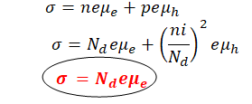
The conductivity of semiconductor is given by:- 


So the concentration is mainly due to mobility of electrons in n-type semiconductor.

So the concentration is mainly due to mobility of electrons in n-type semiconductor.


P-Type semiconductor

When a trivalent impurity likes Boron (B), Al, Ge, In is added to pure Si, a p-type semiconductor is formed. The valence electron of these impurities can form only three complete covalent bonds with silicon which has four valance electrons there is deficiency of one electron to four bonds. This give rise to holes.  In this type of semiconductor the concentration of hole increases with every add of impurities so is called positive type of semiconductor (P-type). Since trivalent atom creates a hole and this hole has tendency to accept an electrons so trivalent impurities is called as accepter.

Let n & p are electrons and hole in semiconductor Na is accepter concentration. The doping of trivalent impurities will increases the hole concentration in valance band but does not increases the electron concentration in conduction band so.


Therefore in p-type semiconductor hole concentration is nearly equal to accepter concentration
Therefore electron concentration in p-type semiconductor is

In trivalent doping of semiconductor the hole concentration increases and electron concentration decreases. This means the minority charger carrier are suppressed by majority charge carriers. This phenomenon is called minority carriers suppression.

Importance of Fermi –energy level:

  • ð  For intrinsic semi conductor Fermi energy level.
  • ð  It is important for4 understanding and determining electric and thermal properties of certain material.
  • ð  They allows us to make calculation as to the density of electron and holes in material or relative amount of each depending on temperature.
  • ð  This is crucial to our understanding of current flow throw semiconductor.
  • ð  In metals the Fermi energy gives us information about velocity of electrons which participates in ordinary electron conduction.
  • ð  For metals the density of conduction electrons can be implied from the Fermi energy
  • ð  It is used to describe insulators metals and semiconductors
  • ð  The Fermi level play an important role in bond theory of solids
  • ð  In doped semiconductor p-type and n-type, the Fermi level is shifted by the impurities illustrated by their band gaps.

Compensation doping:-

It is a term used to describe the doping of semiconductor with both donors and accepters to control the properties. The effect of donors compensates for the effect of accepters and vice-versa.

For eg:-

                A  p-type semiconductor Na accepter can be converted to an n-type semiconductor by simply adding donor until concentration Nd exceeds Na . The holes due to accepter doping will recombine with electron due to donor doping.

Similarly a n-type semiconductor doped with Nd donor can be converted to P-type semiconductor by simply adding acceptor until concentration Na exceeds Nd. The electron due to donor doping will recombines with holes due to accepter doping so the hole concentration is 

notepulchowkcampus.blogspot.com

Similarly a n-type semiconductor doped with Nd donor can be converted to P-type semiconductor by simply adding acceptor until concentration Na exceeds Nd. The electron due to donor doping will recombines with holes due to accepter doping so the hole concentration is
p=Na-Nd
From mass action law,
n.p=ni2
Therefore , the electron Concentration is given by  

notepulchowkcampus.blogspot.com

Where ni=intrinsic concentration

Temperature dependence of carrier concentration:-

Intrinsic concentration of semi conductor is given by :- 

notepulchowkcampus.blogspot.com

Equation (1) implies that electrons and holes concentration in intrinsic semiconductors are the functions of energy band gap and temperature of sample. Both Nc and Nv have T^(3/2) in their expression .So they are also the function of temperature. Since there is negative sign in exponential term it signifies that the increase in band gap will reduce intrinsic concentration and vice-versa. Both from the exponential term Nc and Nv   it can be observed that the increase in temperature will cause increase in concentration as well. The energy band gap is built in characteristics of all material which cannot be altered. Whereas the temperature of sample can be controlled to suit or purpose.

a.)    Low temperature range(T<Ts)

ð  As the temperature is increased starting from very low temperature. Some of donors becomes ionized and donates the electrons to conduction band as shown in figure-1 . The silicon-silicon bond breaking i.e. thermal excitation from valance band to conduction  is difficult because it takes too much energy. The donor ionizations continues until we reach a temperature called saturation temperature(Ts). where all donor atoms have been ionized. This temperature range up to Ts is called ionization range.  


Share:

Electrical Engineering Material Third semester

Infinite Potential Well

https://notepulchowkcampus.blogspot.com/
Engineering stimulates the mind.

Q.1: Starting from the suitable equation, prove that the energy of an electron that is confined in an infinite potential well of width 'L' is quantize (2075 Chaitra BEl 2 year-First Pert(II/I). 

Q.1.b) Prove that the energy of a particle confined in an infinite potential well is quantized. Also, find the expression for the normalized wave function(Regular II/I BEL.BEX 2074 Chaitra)[8 marks]


Electrical Engineering Material (EE502)

Let us consider an electron is confined in a region defined by 0<x<L; where ‘L’ denotes the width of infinite potential well in which an electron is confined.
The potential can be defined as :
V(x) = 0;  at 0 <x< L
V(x) = ∞;  at L <x< 0
It is seen that the potential energy of the particles inside the well is zero and infinite outside the well. Thus the electron inside the well needs infinite potential energy to leave the well hence particles cannot leave the well.
Schrodinger wave equation is
Electrical Engineering Material (EE502)

But inside the well  V = 0
Electrical Engineering Material (EE502)

Where 
Electrical Engineering Material (EE502)

The solution of eq(1) can be written as
Electrical Engineering Material (EE502)

Where A and B are constants whose values are to be determined by using boundary conditions.
Electrical Engineering Material (EE502)

Here A is constants so A can’t be zero so, sine must be Zero
Electrical Engineering Material (EE502)

Electrical Engineering Material (EE502)
From eq(2) and eq(4), we can write
Electrical Engineering Material (EE502)

Here E is the total energy of the electron when potential energy is equal to Zero.
Electrical Engineering Material (EE502)

The energy of the electron that is confined in the region of an infinite potential well cannot be arbitrary nut must be defined by the parameter ’n’. Alternatively, the energy of an electron confined in an infinite potential well is quantize.   

Extrinsic Semiconductor

The conductivity of semiconductor risen when some element belonging to either group iii or group v in Mendeleev periodic table are added on it. These elements are called impurities. The extrinsic semiconductors doped with these impurities is called extrinsic semiconductor. These conductor are of two type :
  1. P- Type semiconductor
  2. N- Type semiconductor

N –Type semiconductor:

When a pentavalent impurity like Arsenic, Potassium, and Antimony is added to a pure semiconductor a n-type semiconductor is formed. The four electrons out of five valance electron of these impurities make covalent bond with four valance electron of si so one electron remains free on every add of impurities. This extra electron continuously revolves around the impurities in core.

                                                                                In this type of semiconductor the concentration of electron increases with every add of impurities so it is called negative type(n-type) semiconductor since the pentavalent atom donate electrons for conduction so it is called donor. In n-type semiconductor e- are majority charge carrier and holes are minty charge carrier.  If n and p represents extrinsic electron and hole concentration of semiconductor. The donor concentration then supposing all donor side are ionized. 

 P-Type semiconductor

When a trivalent impurity likes Boron (B), Al, Ge, In is added to pure Si, a p-type semiconductor is formed. The valence electron of these impurities can form only three complete covalent bonds with silicon which has four valance electrons there is deficiency of one electron to four bonds. This give rise to holes.  In this type of semiconductor the concentration of hole increases with every add of impurities so is called positive type of semiconductor (P-type). Since trivalent atom creates a hole and this hole has tendency to accept an electrons so trivalent impurities is called as accepter.

Let n & p are electrons and hole in semiconductor Na is accepter concentration. The doping of trivalent impurities will increases the hole concentration in valance band but does not increases the electron concentration in conduction band so.

Importance of Fermi –energy level:

  1. For intrinsic semi conductor Fermi energy level.
  2. It is important for4 understanding and determining electric and thermal properties of certain material.
  3. They allows us to make calculation as to the density of electron and holes in material or relative amount of each depending on temperature.
  4. This is crucial to our understanding of current flow throw semiconductor.
  5. In metals the Fermi energy gives us information about velocity of electrons which participates in ordinary electron conduction.
  6. For metals the density of conduction electrons can be implied from the Fermi energy
  7. It is used to describe insulators metals and semiconductors
  8. The Fermi level play an important role in bond theory of solids
  9. In doped semiconductor p-type and n-type, the Fermi level is shifted by the impurities illustrated by their band gaps.


PN- Junction:

In n-type semiconductor electron are majority charge carrier and holes are minority charge carriers and in p-type semiconductor holes are majority charge carrier and electrons are minority charge carriers.

                                when we bring p-type semiconductor in contact with n-type semiconductor then there form an abrupt discontinuity at the junction. This abrupt junction is known as metallurgical junction.

If there two n-type and p-type semiconductor are brought together to form a junction  

Type of polarization

1.       Electronic polarization

2.       Ionic polarization

3.       Dipole orientation polarization

4.       Interfacial polarization

Electronic Polarization  

In an atom in an absence of electric field both charge center lies at same point so there is no polarization but if the external field is applied electron cloud move toward the opposite of applied field and charge separates so there is polarization and induced dipole moment . This type of polarization is known as electronic polarization.   

Induced dipole moment is given by :-

Pind =

the actual field experienced by dielectric material in between capacitor plate is called local electric field . it depends not only on the free charge of the capacitor plate but also on the polarization. In a material of a cubic structure local electric field is given by


For more, please visit by most popular searches
  • engineering notes nepal : Find here most important and useful for short time
  • ioe civil engineering notes
  • pulchowk campus notes
  • ioe solutions
  • engineering mathematics 2 pdf ioe
  • solution of engineering mathematics volume 2 ioe
  • civil engineering notes nepal

Share:

subscribe

IOE ALL SUB NOTES

Delivered by FeedBurner

Wikipedia

Search results

The quality of being the only one of its kind.

If you are fresher or preparing to attempt the Back Exam then you are going to be happy to know that here you will find all the shortlisted targeted question for your subject. Here you will find perfect answers to your questions