Electrical Engineering material(ii/i) ioe ALL SUBJECT NOTE notes
 |
| Download this note in pdf format Click on Download |
Extrinsic Semiconductor
The
conductivity of semiconductor risen when some element belonging to either group
iii or group v in Mendeleev periodic table are added on it. These elements are
called impurities. The extrinsic semiconductors doped with these impurities is
called extrinsic semiconductor. These conductor are of two type :
- 1.
P- Type
semiconductor
- 2.
N- Type
semiconductor
N –Type semiconductor:
When a
pentavalent impurity like Arsenic, Potassium, and Antimony is added to a pure
semiconductor a n-type semiconductor is formed. The four electrons out of five
valance electron of these impurities make covalent bond with four valance
electron of si so one electron remains free on every add of impurities. This
extra electron continuously revolves around the impurities in core.
In
this type of semiconductor the concentration of electron increases with every
add of impurities so it is called negative type(n-type) semiconductor since the
pentavalent atom donate electrons for conduction so it is called donor. In n-type
semiconductor e- are majority charge carrier and holes are minty
charge carrier.
If
n and p represents extrinsic electron and hole concentration of semiconductor.
The donor concentration then supposing all donor side are ionized.
The hole
concentration in n-type semiconductor is less then the extrinsic hole
concentration. This is because some electrons in conduction band recombines
with holes in valance band so as to maintain n.p=ni2. As we go an
increasing concentration of donor atoms there by increasing majority carrier
concentration. The munity carrier concentration will be decreased simultaneously
this is called minty carriers suppressions.
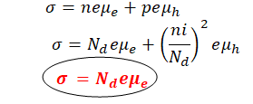
The
conductivity of semiconductor is given by:-
So the concentration is mainly due to mobility of electrons in n-type semiconductor.
P-Type semiconductor
When a
trivalent impurity likes Boron (B), Al, Ge, In is added to pure Si, a p-type
semiconductor is formed. The valence electron of these impurities can form only
three complete covalent bonds with silicon which has four valance electrons
there is deficiency of one electron to four bonds. This give rise to
holes. In this type of semiconductor the
concentration of hole increases with every add of impurities so is called
positive type of semiconductor (P-type). Since trivalent atom creates a hole
and this hole has tendency to accept an electrons so trivalent impurities is
called as accepter.
Let n & p are electrons and hole in
semiconductor Na is accepter concentration. The doping of trivalent impurities
will increases the hole concentration in valance band but does not increases
the electron concentration in conduction band so.
Therefore in p-type semiconductor hole concentration is nearly equal to accepter concentration
In trivalent doping of semiconductor the
hole concentration increases and electron concentration decreases. This means
the minority charger carrier are suppressed by majority charge carriers. This
phenomenon is called minority carriers suppression.
Importance of
Fermi –energy level:
- ð For intrinsic semi conductor Fermi energy
level.
- ð It is important for4 understanding and
determining electric and thermal properties of certain material.
- ð They allows us to make calculation as to
the density of electron and holes in material or relative amount of each
depending on temperature.
- ð This is crucial to our understanding of
current flow throw semiconductor.
- ð In metals the Fermi energy gives us
information about velocity of electrons which participates in ordinary electron
conduction.
- ð For metals the density of conduction
electrons can be implied from the Fermi energy
- ð It is used to describe insulators metals
and semiconductors
- ð The Fermi level play an important role
in bond theory of solids
- ð In doped semiconductor p-type and
n-type, the Fermi level is shifted by the impurities illustrated by their band
gaps.
Compensation
doping:-
It is a term used to describe the doping of
semiconductor with both donors and accepters to control the properties. The
effect of donors compensates for the effect of accepters and vice-versa.
For eg:-
A p-type semiconductor Na accepter
can be converted to an n-type semiconductor by simply adding donor until
concentration Nd exceeds Na . The holes due to accepter
doping will recombine with electron due to donor doping.
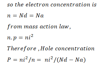
Similarly a n-type semiconductor doped with Nd donor can be converted to P-type semiconductor by simply adding acceptor until concentration Na exceeds Nd. The electron due to donor doping will recombines with holes due to accepter doping so the hole concentration is
Similarly a n-type semiconductor doped with Nd donor can be converted to P-type semiconductor by simply adding acceptor until concentration Na exceeds Nd. The electron due to donor doping will recombines with holes due to accepter doping so the hole concentration isp=Na-Nd
From mass action law,
n.p=ni2
Where ni=intrinsic concentration
Temperature dependence of carrier concentration:-
Intrinsic concentration of semi conductor is given by :-
Equation (1) implies that electrons and holes concentration
in intrinsic semiconductors are the functions of energy band gap and
temperature of sample. Both Nc
a.) Low temperature range(T<Ts)
ð As the temperature is increased starting from very low temperature. Some of donors becomes ionized and donates the electrons to conduction band as shown in figure-1 . The silicon-silicon bond breaking i.e. thermal excitation from valance band to conduction is difficult because it takes too much energy. The donor ionizations continues until we reach a temperature called saturation temperature(Ts). where all donor atoms have been ionized. This temperature range up to Ts is called ionization range.


Grey Structure House Process
ReplyDeleteElectrical Material