Store Program Concept 8085 8086 Microprocessor II/II IOE All Subject Notes
 |
According to this concept the program instruction are stored in memory along side data in a binary number format. Then the computer could get the instructions by reading them from the memory and program could be set or altered by changing the binary values. This approach is known as store program concept and such architecture is known as Von Neumann architecture.
- MBR(Memory buffer resistor):- it consist of the word that is to be stored in the memory or send to I/O unit.
- MAR(memory address resistor):- it contain the address of word that is to be written into or read from MBR.
- IR(instruction resistor):- it contain the opcode of the instruction to be executed.
- IBR(Instruction buffer resistor):- it is temporary resistor that holds the right hand instruction from a word in the memory.
- PC(Program counter):- It contains the address of next instruction to be fetched from the memory.
- Accumulator and multiplier Quotient(AC & MQ):- it holds the operands and results of ALU after processing.
Architecture of computer
Every object in the world has its own architecture like human has its body architecture even building and offices has its own architecture. Architecture defines how function works the same way computer has architecture on which computer runs .
There are two types architecture
- von Neumann architecture
- Harvard architecture
Working of Von Neumann architecture
von Neumann architecture was designed and developed by the great mathematician and scientist John von Neumann in the year 1945s most of the computer of today's world run on the von Neumann architecture whether mainframe or personal computer .
the input or instruction comes in and stores in the memory the input becomes the command and ready to process the processor fetched the command from memory there is two part in the process
- control unit
- ALU arithmetic logic unit
component of von Neumann architecture
- input :- it comes through input device like keyboard mouse etc.
- memory:- the data are temporary store in the memory called RAM
- process:-process has two parts one control unit the control units it control and manage the process and input/output the control unit fetch and store data to and from memory - another arithmetic logic unit the role of the ALU is to perform mathematics calculation like addition subtraction multiplication/division etc
- output:- the output display through the monitor printer etc.
Q1. Explain fetch and execution cycle of an instruction of a stored program computer. Illustrate with the help of RTL specification.
Ans:-The fetch and execution cycle is the basic operation (instruction) cycle of a computer. During the fetch and execute cycle the computer retrieves a computer program instruction from its memory. It then establish and carriers out the actions that are required for that instruction.
It consist of the following steps;-
8086 Architecture (40 pin IC)
 |
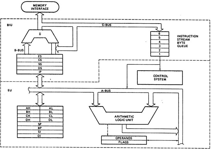
| 8086 internal architecture |
The architecture of 8086 is divided into 2 functional unit :-
- BIU→Bus interface Unit
- EU→Execution unit
Bus interface unit:
- It fetches the instructions or data from memory
- write data to memory
- Read/ write data to I/O port
- Instruction pointer(IP)
- segment registers
- instruction queue
1.Instruction pointer: (IP)
It is 16 bit register that keeps the address of memory location of next coming instruction to be executed.(i.e. address of next instruction)
2.Segment Registers:
The memory space 1MB of 8086 is segmented into following four blocks.
- code segment(CS) 👉 code segment contains the instruction that are to be executed. CS register addresses the code segment.
- data segment(DS)👉 it contains the program define data, constants, etc. DS register addresses data segment.
- stack segment(SS)👉it contains any data and address that the program needed to save temporarily or for subroutine. SS register addresses stack segment.
- extra segment(ES)👉it contains extra data or program that are not accommodated in previous segment. ES register addresses extra segment.
3.Instruction Queue
BIU fetches the instruction byte while execution unit is executing operation. The prefetched instruction is saved in the group of high speed registers which is known as queue. It is of 6 bytes. The instruction codes are prefetched from the memory a head of the time so that there is always queue of instruction ready to execute. This mechanism is known as pipelining which speed up the processing task.
Execution unit(EU)
Functions:-
- It decodes and execute the instructions that have been fetched by BIU
- General purpose registers (GPRS)
- pointer and index register
- ALU
- Flag register
- Timing and control unit
General Purpose Registers(GPRS):
8086 contains 4 general purpose registers which are of 16 bit.
- AX: In and out instruction uses accumulator for input output and mostly arithmetic operation.
- BX: Base register used also for addressing besides computation.
- CX: Count register used for looping and computation purpose
- DX: data register for normal computation especially for multiplication and division. When AX and DX are used as pair.
Pointer and Index Register:
8086 has two pointer and 2 index register.
- SP → stack pointer
- BP → base pointer
- SI → source index
- DI → destination index
Flag registers: It is 16 bit register among which 9 flags are used and remaining 7 flags are unused
9 flags are divided into two group
- status flag : it contains 6 flags (i.e. Over flow , sign, zero, auxiliary carry, parity, carry flags)
- control flag : it contains 3 flags(i.e. directional, interrupt enable, Trap flags)
 |
| 8086 MP Flags |
- Over flow flag (OF): it is set if there is carry from MSB.
- Directional flag(DF): it is used for string processing for moving or comparing string characters. 1 indicate right to left and 0 indicate left to right.
- Interrupt flag(IF): 8086 react to interrupt form external device if it is set to 1.
- Trap flag(TF): if TF is set to 1 the processor runs on single step mode.
Q. Explain the process of assembling linking and executing assembly language program.
 |
| Steps in assembling linking and executing ASM |
Assembler:
- Convert source program into object program and generate .obj file.
- Calculate off set address of data items in data segment and instruction in code segment.
- it generates .ltr and .crf file which are optional that can be generated during runtime.
- assembler reads each line of instruction as ASCII character and translate them into their respective machine code.
- assembler also complain about syntax error if any.
Linking
- it involves converting of object module (.obj) into machine executable code i.e .exe.
- it completes the address left by assembler.
- it combines separately assembled object files.
- it creates .EXE, .LIB, .MAP files and .LIB, .MAP files are optional.
loading and executing
- load the program into memory for the execution.
- resolve the reaming address.
- create the program segment prefix (PSP) before loading.
- execute the program to generate the result.
Difference between one pass and two pass assembler is given below
Write short note on DSP.
- It is special type of CPU which provides ultra fast instruction sequence such as shift and add, multiply and add these are mostly used for intense signal processing.
- DSP work with digital signal only so any analogy signal must be converted before using in DSP so there is requirement of ADC and DAC for displaying digital signal into analogy form.
- Various DSP function can be implemented by using software and hardware. Software implementation is slow and hardware implementation required different architecture other than von Neumann.
- DSP is based on Harvard architecture where data and program are stored separately so processing speed of processor is super.
- They are target to special application such as audio card, video card, Fourier transform (FTT), etc.
- specialized addressing mode.
- single cycle –multiply accumulator capability
- Motorola 3600


* address memory module
ReplyDeleteThank you we have made correction
Delete